Learning Objectives
- Understand how feeding an output to an input provides a memory element.
- Understand and be able to build a SR-latch and a D-latch.
- Understand the difference between level triggers and edge triggers.
- Understand the difference between latches and flip-flops.
- Understand what a finite-state machine is and what elements are in a state machine.
- Be able to build a finite-state machine from a set of inputs.
Recall that combinational logic produces an output based on a set of inputs. Sequential logic is much like this except now it considers a previous output. That is, sequential logic produces an output based on a set of inputs AND outputs. We generally use sequential logic to delay a circuit or to store values. For example, registers are made up of sequential circuits.
You will easily be able to identify a sequential circuit when an output of one gate feeds back into its input. Here's an example of a sequential logic circuit:
Using the circuit above, we use the output (Q) as an input to the OR gate, which then feeds back into the AND gate. Whenever SET and CLEAR are both 0, this circuit remembers what the last operation was. If we make SET=1 and CLEAR=0, then the output becomes 1. If we make SET=0 and CLEAR=1, then the output becomes 0. You can see that if SET=1 and CLEAR=1 that the bottom input of the AND gate will become 0, and hence set the output to 0. Here are the multiple ways this circuit can be executed.
Triggering
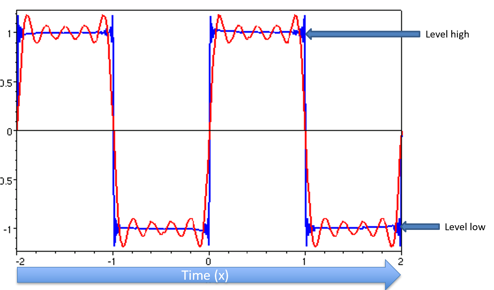
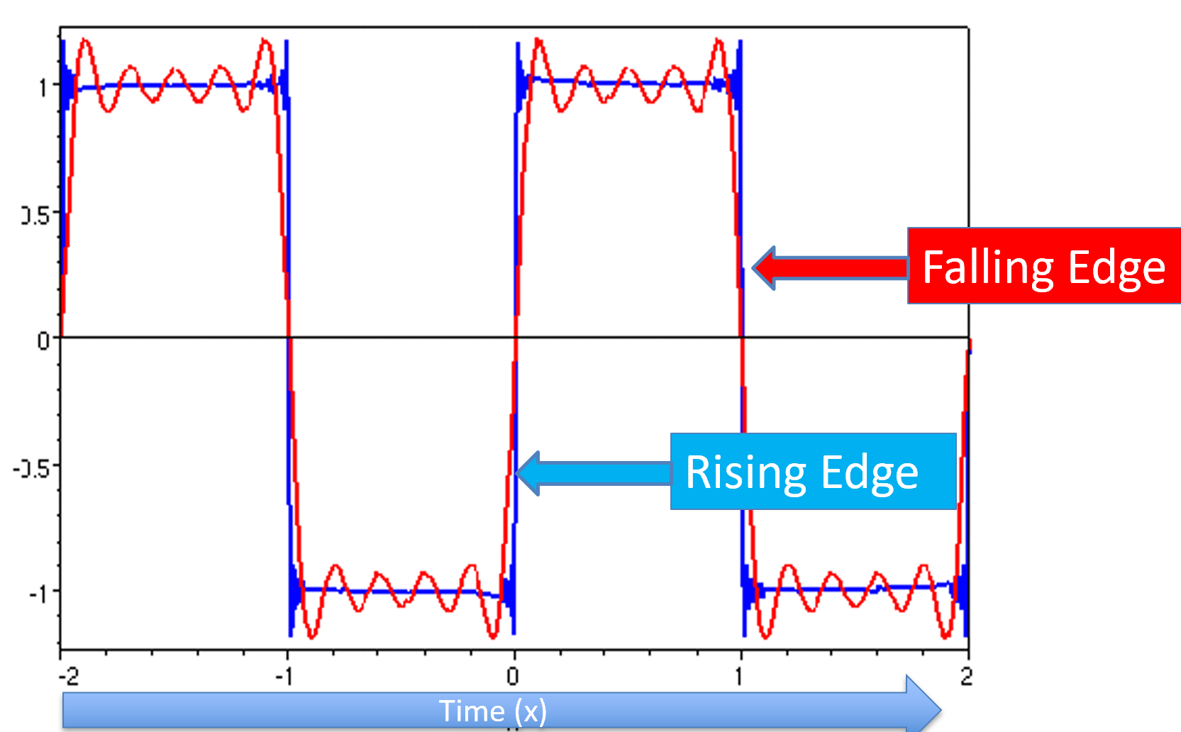
Since sequential circuits can remember a value, we need to be able to control when this "remembering" takes place. When the output flips due to a change in input, it is called a trigger. There are four ways a sequential circuit can be triggered: (1) level-high, (2) level-low, (3) rising-edge, and (4) falling-edge. A level trigger will trigger whenever the input pin is at a given level. Level-high would mean that the input pin is 1, level-low would mean that the input pin is 0. An edge trigger requires a transition. A rising-edge means that a pin went from 0 to 1. A falling-edge means that a pin went from 1 to 0.
Sequential circuits that are level-triggered are called latches (remember Level/Latch both start with L), whereas edge-triggered sequential circuits are called flip-flops.
The following diagram depicts an oscilloscope view of a level trigger.
An edge trigger requires a transition. The following diagram depicts rising and falling edges.
The triggers are transitions from an input. These can be from a simple input pin, the output of a logic gate, or even a clock. A clock is defined as something that generates an output of 0 to 1 and back to 0 within a certain amount of time. That amount of time is measured in HZ (Hertz), which means "times per second". For example, 2 HZ would mean that the clock generates 0 to 1 back to 0 twice within a second. 1 HZ would mean that it generates 0 to 1 back to 0 once within a second. This is called the clock frequency. As you can see, you could easily do this yourself if you had a simple input pin. For 1 Hz, you would flip the input from 0 to 1 within a half of a second, then flip it from 1 back to 0 within the other half of a second.
Latches
Recall that latches are level-triggered. This means as soon as we set a pin, the output will change. It doesn't require a transition from 0 to 1 or 1 to 0.
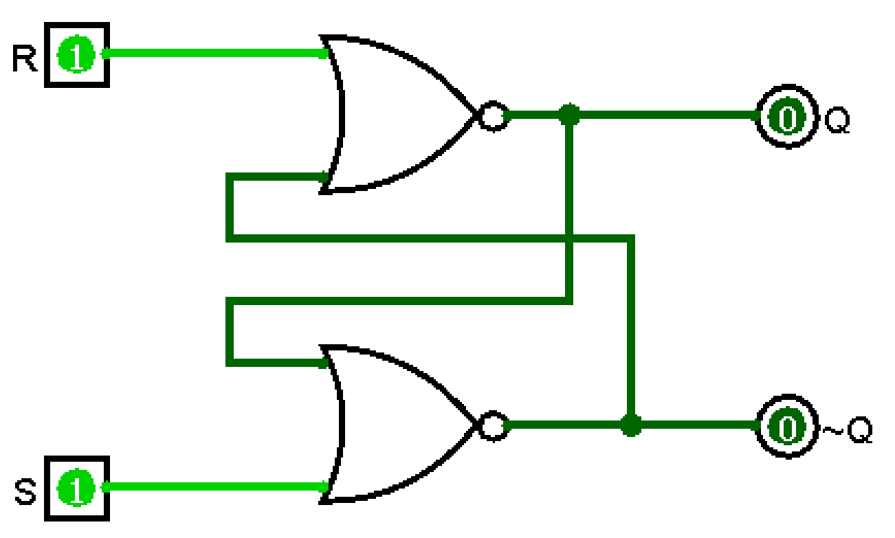
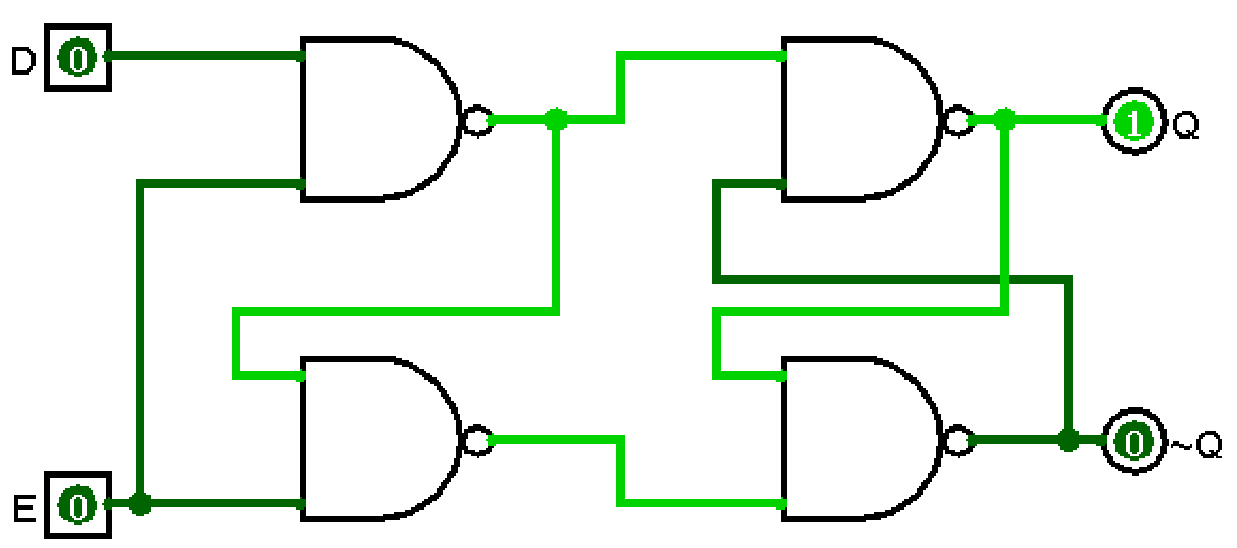
The SR-latch (set/reset)
An SR (set/reset) latch operates much like the circuit above. When we make S=1, the output becomes 1. When we make R=1, the output becomes 0. If S=0 and R=0, then the output remembers the previous operation. An SR-latch looks as follows.
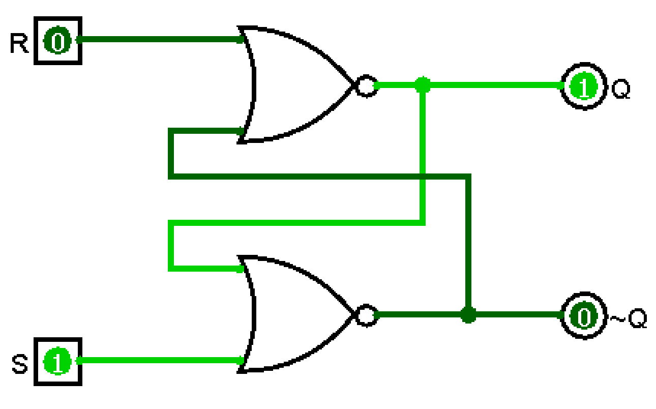
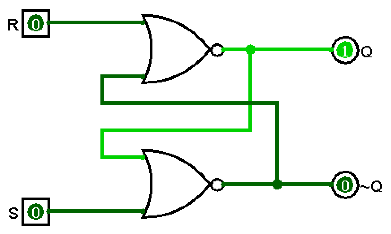
The SR-latch has both outputs \(Q\) and \(\neg Q\), but you can see that when S=1, it takes the output of 1. When R=1, it takes the output of 0. Whenever S=0 and R=0, it remembers the previous value. For SR-latches, S=1 and R=1 is considered undefined.
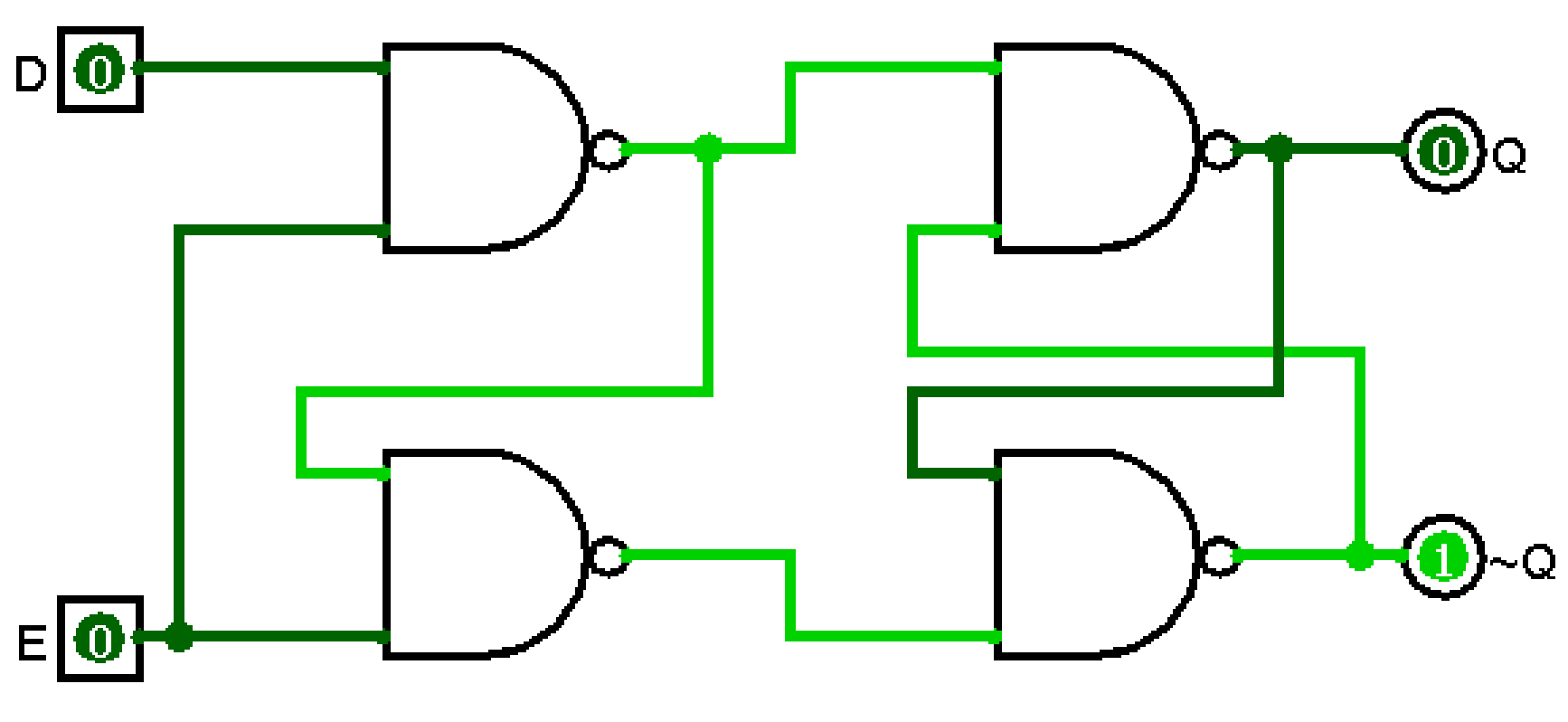
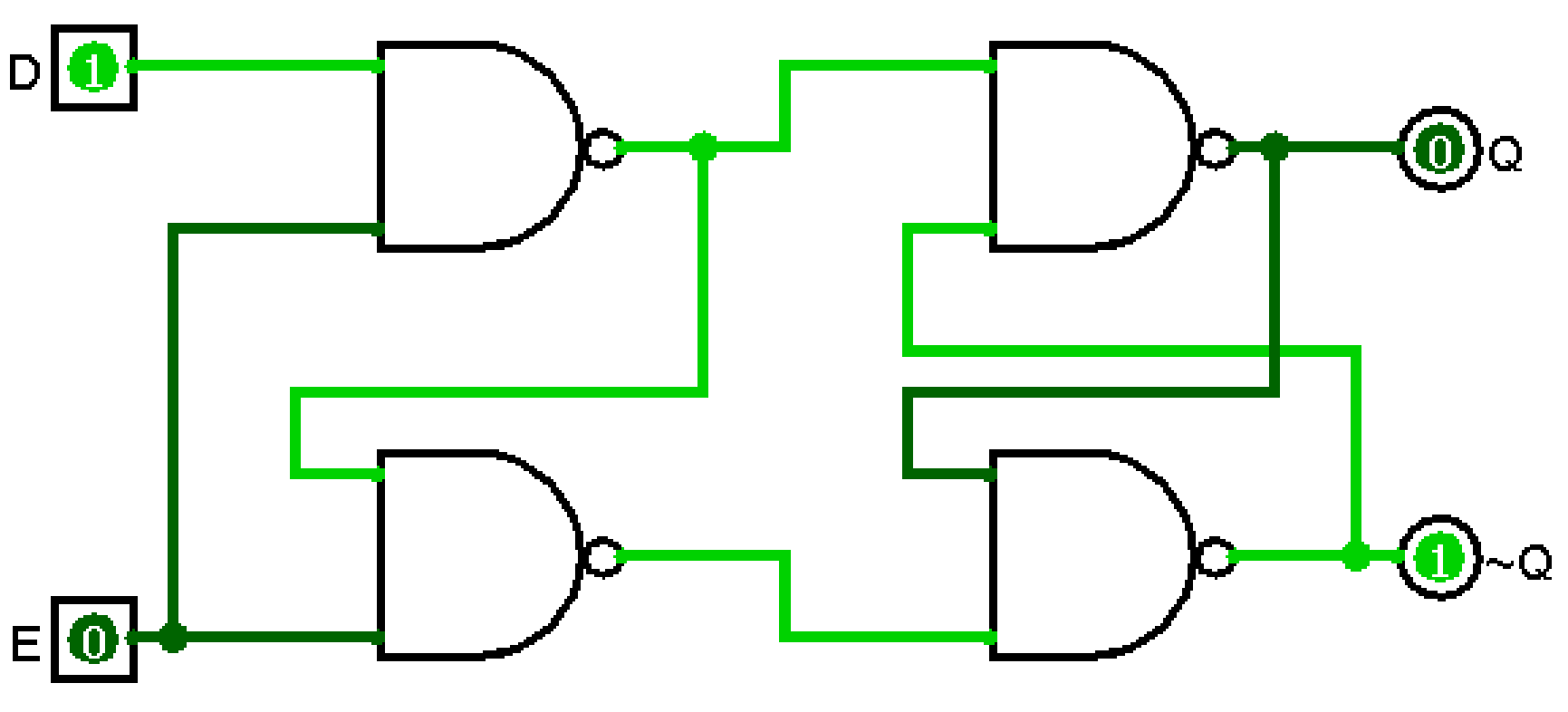
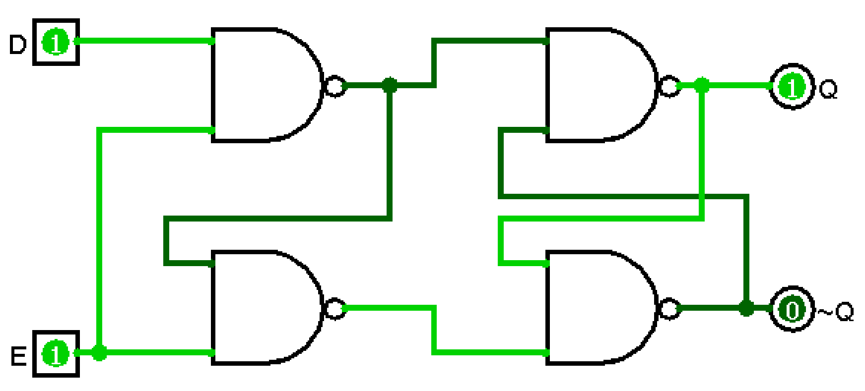
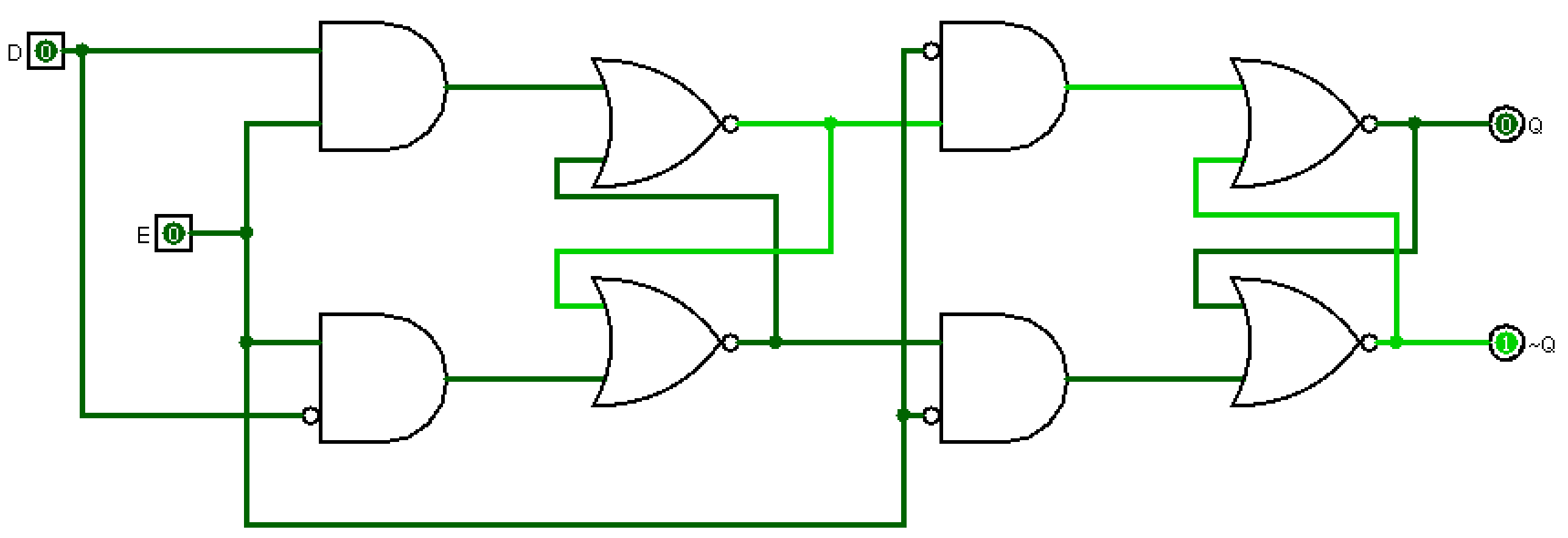
The D-latch (data latch)
For the SR-latch, we used one pin to set the data and one to clear the data. However, what if we want one pin to be the data, and the other to be whether to remember or take the value of the data? This is the concept behind a D latch. We have two pins D (data) and E (enable). When E=0, the latch remembers the previous value regardless of D. When E=1, the latch takes whatever value is in D. Here's a truth table for the D-latch.
| D (data) | E (enable) | Q (output) |
|---|---|---|
| 0 | 0 | Previous Q |
| 0 | 1 | 0 |
| 1 | 0 | Previous Q |
| 1 | 1 | 1 |
As you can see above, as long a E=0, then we remember the previous value. We use the D-latch for registers. We have some sort of data that we want to remember, so we set D=data and then toggle E=0, E=1, E=0. Since E goes back to 0, we can then set D to whatever we want, and the latch will still remember the previous value. The circuit diagram of a D-latch is below.
Flip-flops
Latches only consider the input pins and the previous outputs. A flip-flop requires a certain transition from 0 to 1 (rising edge) or from 1 to 0 (falling edge). This is why we call flip-flops edge-triggered. These circuits are a little bit more involved, but the following circuit diagram depicts a D-flip-flop (NOT a D-latch).
This is a falling-edge triggered D-flip-flop. I did warn you it was more involved. If we wanted a rising-edge triggered D-flip-flop, we would just invert the E (enable) pin.
In the D-flip-flop above, Q will only take the value of D when E=1 and then goes to E=0. The opposite isn't true. If D=1, and E goes from 0 to 1, the output (Q) does not change, and it will stay 0 given the conditions above.
Registers
Recall that in MIPS, we used registers. Registers are usually a set of D-latches. The reason we have a different term for them is because a D-latch stores only 1 bit. So, for a 32-bit register, we need 32 D-latches side by side--one for each bit.
When you hear "registers", you should be thinking of sequential logic.
Finite State Machines (FSM)
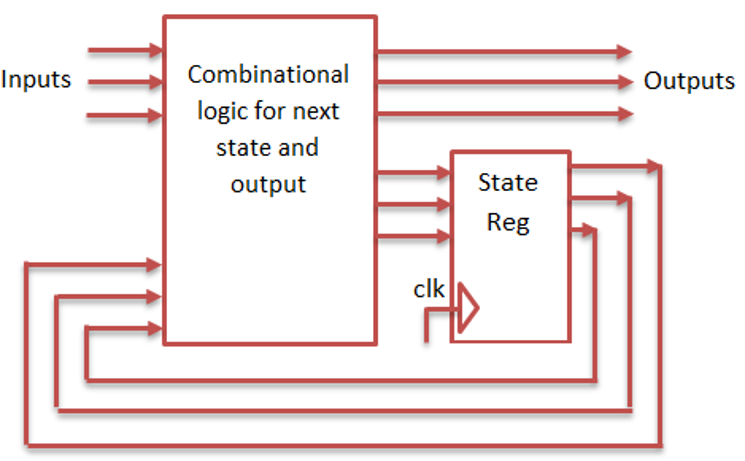
It gets tough to depict sequential circuits using just a truth table, since there is not concept of "time". A finite state machine (FSM) is a diagram that depicts transitioning through a set of states (hence the name). We need 1 bit to store at most 2 states. So, if we need 14 states, we need \(2^4=16\), 4 bits. That gives us 16 states, but we just don't use the last two states.
Finite state machines contain two elements: (1) combinational logic and (2) state registers. The combinational logic takes the current state and other inputs and determines what the next state is. The state registers just store the current state. Remember, we need \(\log_2{\text{states}}\) number of latches or flip-flops to store the state.
It is important to know which type of sequential circuit to use for a finite state machine. This affects the behavior of your FSM. If we use a falling edge D-flip-flop to store the states, we don't transition until some bit goes from 1 to 0. The transition will NOT take place if we go from 0 to 1, since that would be a rising-edge.
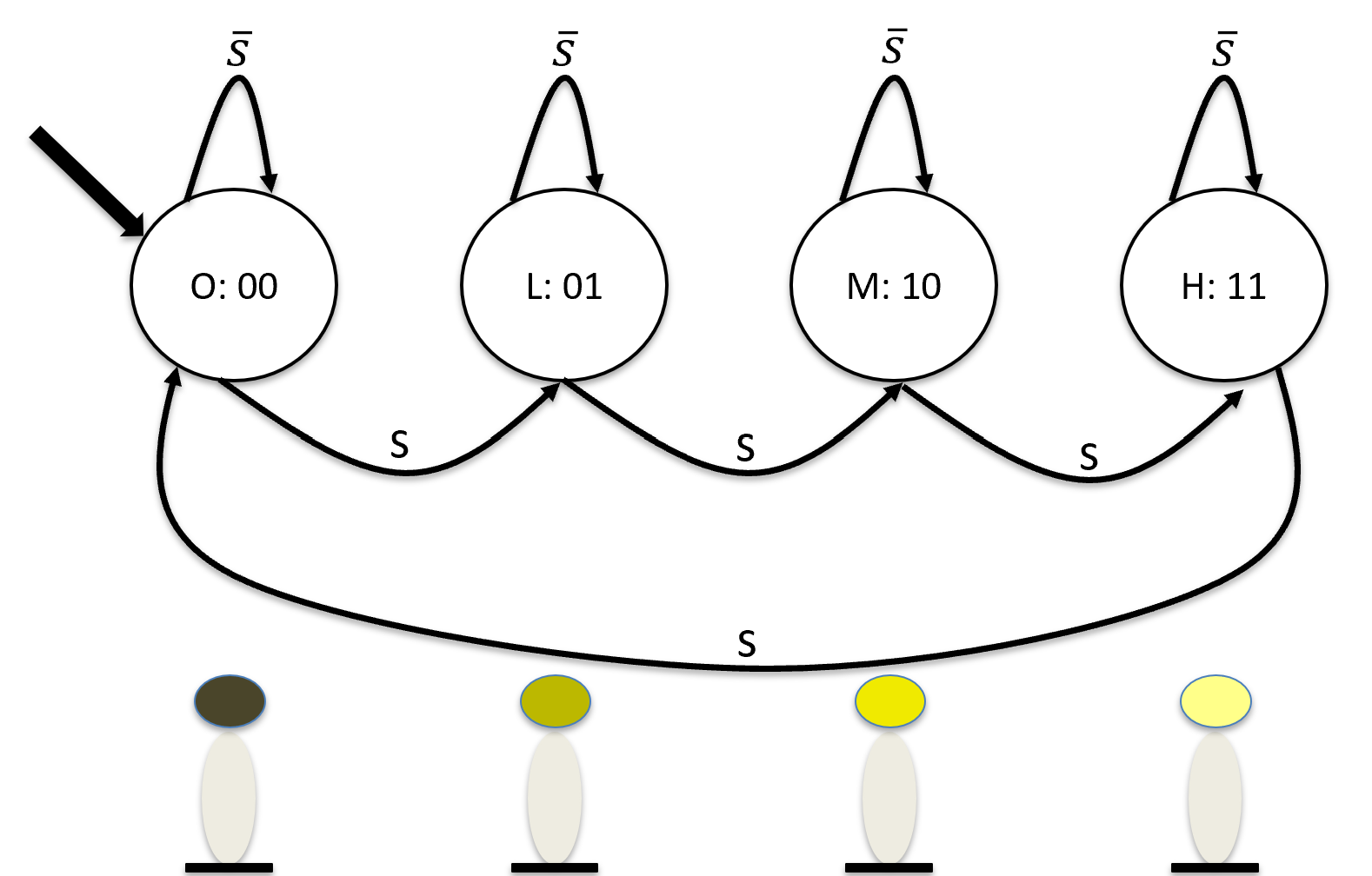
As an example, let's consider a lamp with a 3-way bulb. The bulb has two filaments (L) low and (M) medium. The (H) high setting is just both L and M illuminated simultaneously. A finite state machine can be depicted as follows.
The diagram depicts a mealy-machine, which is just fancy for a machine whose output depends on the current set of inputs and current state. In this course, we will just call these generally FSMs.
So, now we need to set up our lamp's logic. When we first turn plug it in, the states will be 00 (M=off,L=off). When we press the switch, it completes a circuit and triggers the state to move to 01 (M=off,L=on). Then when we press it again, it completes a circuit and triggers the state to move to 10 (M=on, L=off). If we press it again, the state will move to 11 (M=on, L=on). Finally, if we press it again, the lamp will turn off and move to 00 (M=off, L=off). The following truth table depicts our lamp logic.
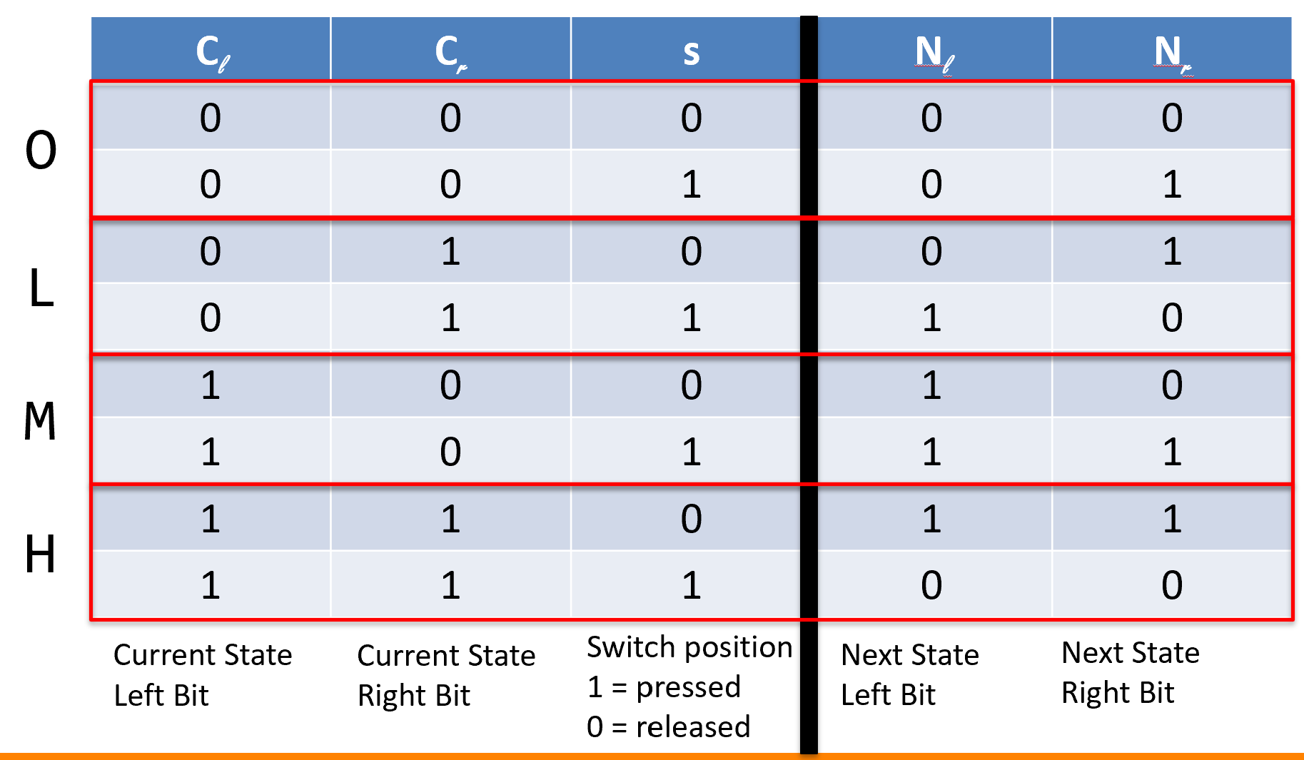
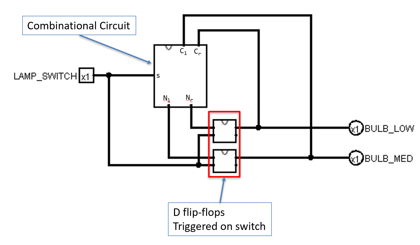
Our combinational logic circuit will contain three inputs: two from the state registers (Cl and Cr for current_left and current_right) and one from the switch. Since our combinational logic controls transitioning to different states, we can use two D-latches to store the state bits. We use latches because if we held the switch down, our combinational logic would keep cycling through modes. Instead, we want it to only switch states when the switch goes from NOT being pressed to being pressed. In other words, when the circuit goes from 0 to 1 (rising-edge).
The following diagram is called a finite state machine diagram. The thick arrow from the left is the "starting point" for our state machine. You can see what causes a transition (the bit s for switch).
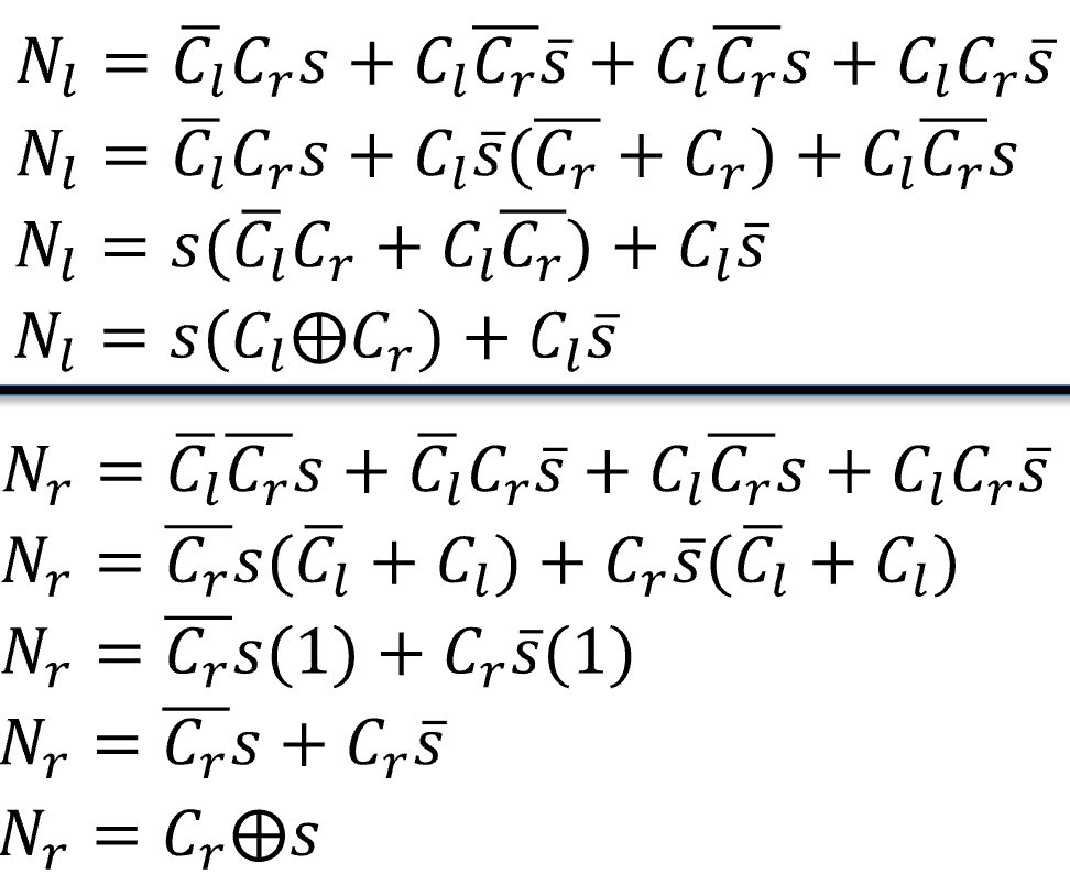
Now, we can use POS or SOP to develop our combinational logic circuit. The state machine is easy, we just need two rising-edge, D-flip-flops, one for Cr and one for Cl. I reduced the equations below to make our circuits easier, but you might not know how to do that, yet.
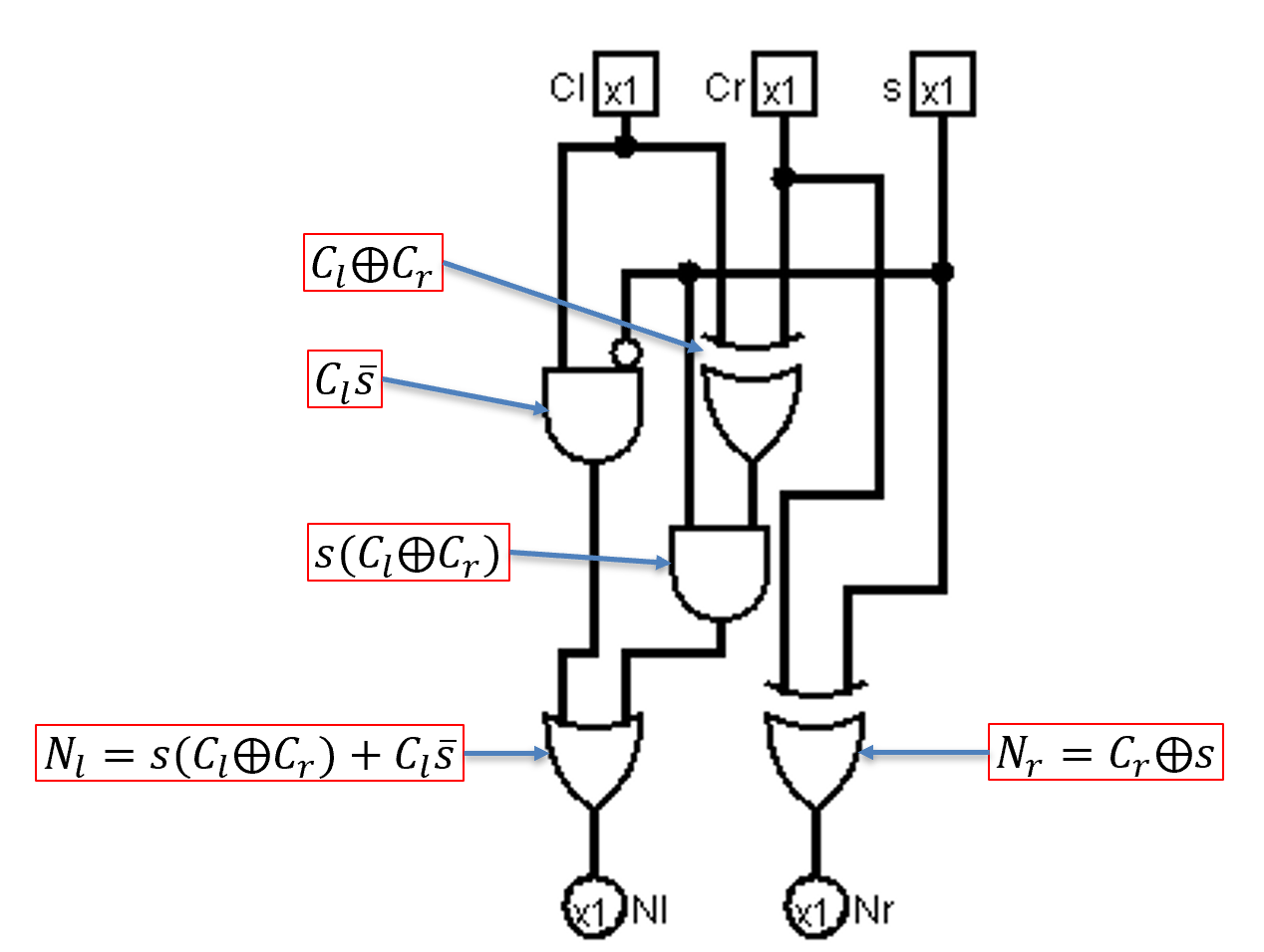
We can then take these equations and draw the circuit diagrams for them.
Now, we link all of this together to including the inputs, outputs, and state registers.
Conclusion
Hopefully, it is becoming clear how we can make routing electrons do actual work for us. We made a simple lamp circuit using digital logic and everything we've learned.